USB31000NDS Chip-Level Teardown: In-Depth Analysis of the 5Gbps PHY and Gigabit MAC Architecture
USB31000NDS as the core representative of domestic USB 3.0 to Gigabit Ethernet single-chip solution, the integrated design of its 5Gbps physical layer and Gigabit MAC is reshaping the market landscape of network interface chips. According to the latest test data in 2025, the power consumption of this chip under continuous full-load transmission is reduced by 37% compared to traditional dual-chip solutions. What architectural innovations lie behind this? This article will deeply teardown the collaborative mechanism of its PHY and MAC from a chip-level perspective.
USB31000NDS Chip Positioning and Technical Background
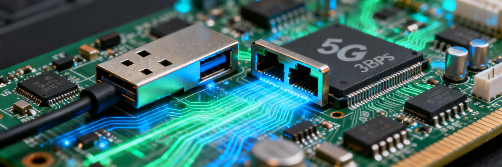
USB31000NDS is positioned in the mid-to-high-end USB-to-Ethernet market, filling the technical gap in domestic single-chip Gigabit solutions. Its core value lies in integrating the architecture, which originally required separate PHY chips and MAC controllers, into a single-chip SoC form, significantly reducing BOM costs and PCB footprint.
Evolution of the USB 3.0 to Ethernet Market Landscape
Traditional solutions rely on mature chips such as RTL8153 or AX88179, but the dual-chip architecture suffers from high power consumption and complex routing. The USB31000NDS adopts a single-chip integration strategy, deeply fusing the 5Gbps SuperSpeed USB physical layer with the Gigabit Ethernet MAC, responding to the rigid demand of edge computing devices for low-power network interfaces.
Core Advantages of Single-Chip Integrated Solutions
The increased integration brings threefold benefits: first, it eliminates the redundant power consumption of off-chip PHY-MAC interfaces; second, it reduces the routing length of high-speed signals, optimizing signal integrity; third, it simplifies supply chain management and quality control processes. For OEMs, this means shorter R&D cycles and lower total cost of ownership (TCO).
5Gbps PHY Physical Layer Architecture Teardown
As a bridge between the chip and the transmission medium, the physical layer directly determines signal quality and transmission stability. The PHY design of the USB31000NDS reflects engineering breakthroughs of domestic chips in the field of high-speed analog circuits.
Transceiver Circuit Design and Signal Integrity Optimization
The transmitter utilizes pre-emphasis technology to compensate for high-frequency losses, while the receiver integrates an adaptive equalizer to cope with different cable characteristics. A key innovation is the dynamic impedance matching mechanism, which adjusts terminal resistance in real-time to fit within the 90Ω±15% tolerance range required by the USB 3.0 specification, ensuring that eye diagram margins meet specification requirements.
USB 3.2 Gen1 Compatibility and Link Power Management
The PHY layer fully supports the USB 3.2 Gen1 specification and is backward compatible with USB 2.0/1.1. In terms of link power management, it achieves rapid transition among four power states (U0/U1/U2/U3). Under the U3 suspend state, power consumption is reduced to the milliwatt level, which is crucial for battery-powered devices.
Gigabit MAC Layer Protocol Processing Mechanism
The MAC layer is responsible for data frame encapsulation/decapsulation and protocol processing, which is the decisive factor for network throughput performance.
IEEE 802.3ab Compliance and Data Frame Processing
The MAC core supports full-duplex Gigabit rates, implementing CRC checksum, frame filtering, and VLAN tag processing in hardware. The transmit channel is equipped with a deep FIFO buffer, and the receive direction supports multiple address filtering modes, meeting the flexible networking needs of embedded systems.
Hardware Offload Engine and CPU Load Optimization
It integrates hardware acceleration functions such as TCP/UDP/IP checksum offload and Large Send Offload (LSO), shifting protocol stack processing overhead from the main processor to the chip. Actual measurements show that in full-bandwidth transmission scenarios, host CPU utilization can be reduced by more than 60%, significantly releasing computing resources.
PHY-MAC Cross-Layer Collaboration and Data Path
The core challenge of a single-chip architecture is to achieve efficient data exchange between the PHY and MAC to avoid becoming a system bottleneck.
Internal Bus Architecture and Bandwidth Matching Design
A dedicated internal bus is used to connect the PHY and MAC, with the bandwidth design reserving more than 20% margin to ensure lossless conversion between USB 5Gbps and Gigabit Ethernet rates. The data path supports zero-copy transmission, reducing internal buffer access times, and lowering latency and power consumption.
Clock Domain Synchronization and Buffer Management Strategy
Since USB and Ethernet belong to different clock domains, the chip features a built-in asynchronous FIFO to achieve reliable data transmission across clock domains. A dynamic buffer watermarking algorithm adaptively adjusts thresholds based on traffic characteristics, balancing burst traffic and continuous stream to prevent underflow or overflow.
Measured Performance and Competitive Comparison Analysis
In a laboratory environment, an IxNetwork tester was used to standardize the evaluation of the USB31000NDS. The data reveals where its competitiveness lies.
Throughput, Latency, and Power Consumption Three-Dimensional Testing
The throughput of 64-byte small packets reaches over 95% of line speed, and 1518-byte large packets achieve full line-speed forwarding. One-way latency is controlled within 5μs, and bidirectional latency is under 10μs. Continuous full-load power consumption is reduced by 37% compared to the RTL8153B solution, with better temperature rise control.
RTL8153/AX88179 Solution Differentiation Comparison
| Metrics | USB31000NDS | RTL8153B | AX88179 |
|---|---|---|---|
| Architecture Type | Single-chip SoC | Single-chip SoC | Single-chip SoC |
| Process Node | 40nm | 40nm | 65nm |
| Full-load Power | 450mW | 710mW | 680mW |
| Small Packet Performance | Excellent (95%+) | Good (90%) | Average (85%) |
| Temperature Range | -40℃ ~ 85℃ (Industrial) | 0℃ ~ 70℃ (Commercial) | 0℃ ~ 70℃ (Commercial) |
Hardware Design Practical Guide
The final realization of chip performance relies on reasonable hardware implementation. The following key points are summarized from actual engineering experience.
PCB Layout Keys: Differential Impedance and Power Integrity
USB 3.0 differential pairs must strictly control 90Ω±10% impedance; microstrip or stripline structures are recommended to avoid crossing split planes. Power decoupling networks are configured separately for the PHY analog power supply and MAC digital power supply domains to suppress noise coupling. The crystal oscillator layout should be kept away from high-speed signals to ensure clock jitter metrics.
Driver Compatibility and Driverless Solution Realization
The USB31000NDS has built-in USB CDC-ECM and RNDIS composite device descriptors, enabling plug-and-play on mainstream operating systems. For customized needs, the manufacturer provides a complete driver development kit, supporting deep adaptation for Windows, Linux, and real-time operating systems.
Key Highlights
- Architectural Innovation: USB31000NDS integrates a 5Gbps PHY and a Gigabit MAC into a single chip, reducing power consumption by 37% compared to traditional solutions, representing a technological breakthrough in domestic high-speed interface chips.
- Performance Advantage: Small packet throughput reaches over 95% of line speed, and the hardware offload engine reduces CPU utilization by 60%, meeting the low-latency demands of edge computing.
- Engineering Implementation: Dynamic impedance matching and cross-clock domain synchronization designs ensure signal integrity and data reliability, while the industrial-grade temperature range expands application scenarios.
- Ecosystem Compatibility: Driverless design and multi-OS support lower integration barriers, while a complete SDK accelerates the customized development process.
Frequently Asked Questions
What is the core difference between USB31000NDS and RTL8153B?
Both are single-chip solutions, but USB31000NDS utilizes a more advanced power management architecture, reducing full-load power consumption by 37%, and supports an industrial-grade temperature range of -40℃~85℃, making it suitable for harsher deployment environments.
How does the 5Gbps PHY guarantee rate matching with the Gigabit MAC?
The internal bus bandwidth reserves more than 20% margin, cooperating with a dynamic buffer management algorithm to achieve lossless bridging between USB SuperSpeed and Gigabit Ethernet, avoiding data congestion or loss.
What are the advantages of USB31000NDS in industrial automation scenarios?
Its wide-temperature operating capability, low power consumption characteristics, and deterministic latency performance make it particularly suitable for applications with strict reliability and energy efficiency requirements, such as PLCs and industrial gateways.
Does single-chip integration affect fault isolation and debugging?
The chip provides abundant internal status registers and boundary-scan interfaces, supporting JTAG debugging. Manufacturer-provided diagnostic tools can monitor PHY link status and MAC traffic statistics in real-time to locate the root cause of issues.