
Driven by Application Scenarios: Why 312.5MHz LVDS Becomes a High-End Standard?
The 312.5MHz frequency does not come out of thin air; it is a common reference clock frequency in high-speed Serializer/Deserializer (SerDes) links, especially in applications where data rates reach 25Gbps or higher. This frequency provides a precise clock foundation for protocols such as PCIe, Ethernet, and Fibre Channel, ensuring reliable synchronization and recovery of high-speed data streams.
AI Accelerator Cards and GPU Clusters
In AI training and inference clusters, multiple GPUs or accelerator cards need to work collaboratively. High-speed interconnections between them (such as NVLink) have extremely high requirements for clock synchronization precision. The 312.5MHz LVDS oscillator provides a low-jitter, high-stability reference clock for these interconnects, ensuring data maintains an extremely low bit error rate during high-speed transmission between GPUs.
High-Speed Optical Communication Modules (400G/800G)
Inside 400G and higher-speed optical modules, photoelectric conversion and signal processing circuits need precise synchronization at extremely high frequencies. The low-phase-noise clock generated by the 312.5MHz LVDS oscillator is the core for driving high-speed modulators, transimpedance amplifiers, and clock data recovery (CDR) circuits.
Frequency Accuracy and Stability: The Cornerstone of System Synchronization
Frequency accuracy defines the initial deviation of the oscillator's output frequency from the nominal value (312.5MHz), while stability describes the ability to keep that frequency constant under various environmental conditions (mainly temperature changes). Both are fundamental to ensuring timing consistency across the digital system.
Phase Noise and Jitter: Signal Purity
For 312.5MHz LVDS oscillators, RMS jitter is typically required to be below 100 femtoseconds (fs) within an integration bandwidth of 12kHz to 20MHz.
Output Logic Comparison
Power Supply and Consumption: Constraints of High-Density Design
The common operating voltage for 312.5MHz LVDS oscillators is 3.3V. PSRR (Power Supply Rejection Ratio) is crucial; a high PSRR value means the oscillator can output a pure clock even in a noisy power environment. Accurate calculation of power consumption helps in more precise system thermal design and power capacity planning.
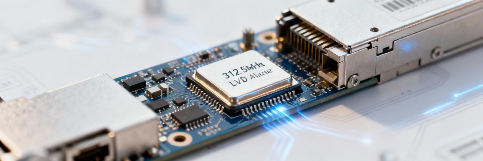
Package and Reliability: 3225 Mainstream Choice
3225 (3.2mm x 2.5mm) is the current mainstream package size. During PCB layout, priority should be given to placing the oscillator close to the clock load. Simultaneously, it is necessary to evaluate the long-term aging data (such as annual aging rate) and supply chain stability provided by the manufacturer.
Practical Selection Process and Pitfall Prevention Guide
Key Summary
- Application Sets the Tone: The 312.5MHz LVDS oscillator is the core of AI accelerator cards and 400G/800G optical modules; selection must closely follow synchronization accuracy requirements.
- Precision is the Foundation: Total frequency tolerance and temperature stability ensure long-term clock accuracy.
- Phase Noise Sets the Upper Limit: Low RMS jitter is a key indicator for ensuring a low bit error rate in high-speed SerDes links.
- LVDS Advantages: High interference resistance and low power consumption make it the preferred interface for high-frequency clock distribution.
- Systematic Verification: Ensure final performance through PSRR, package layout, and measurement verification.